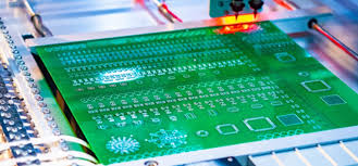
The Backbone of Circuit Design
PCB routing is the process of connecting various components on a circuit board through electrical traces. These traces act as conduits for electrical signals, defining the pathway that allows components like microchips, resistors, and capacitors to interact. The quality of PCB routing directly influences the performance and functionality of the final electronic device.
Enhancing Device Performance and Functionality
Effective routing is crucial for minimizing signal loss and interference. Poorly routed PCBs can suffer from a variety of signal integrity issues, such as crosstalk and noise, which can degrade the performance of sensitive components. For high-speed applications, like in telecommunications equipment, signal integrity becomes even more critical. Designers must ensure trace lengths and widths are precisely calculated to maintain signal integrity. For example, in a high-speed transmission line, keeping impedance within a 10% tolerance of 50 ohms is essential for preventing signal reflection and ensuring stable data transmission.
Mitigating Electromagnetic Interference
One of the main challenges in PCB routing is managing electromagnetic interference (EMI). Designing a PCB layout that minimizes EMI is crucial for compliance with global regulatory standards, such as those set by the Federal Communications Commission (FCC) in the United States. Techniques like using differential pairs for signal traces, where two parallel traces carry inverted signals, can significantly reduce EMI. This technique is particularly effective in applications like USB and Ethernet connections where maintaining signal integrity at high data rates is essential.
Optimizing Real Estate on PCBs
Efficient use of space is another critical aspect of PCB routing. As electronic devices become smaller, the demand for compact, yet highly functional PCBs increases. Effective routing helps in maximizing the utilization of available space. For instance, multilayer PCBs, which can have anywhere from 4 to 12 layers or more, utilize sophisticated routing techniques to overlay multiple layers of traces, optimizing space and enhancing functionality.
Cost Reduction Through Smart Design
Strategic PCB routing also plays a significant role in reducing production costs. By optimizing the layout to use fewer materials, such as less copper for traces, and minimizing the number of vias (holes that connect different layers of a PCB), manufacturers can significantly reduce costs. Additionally, well-planned routing can decrease the need for later modifications or corrections, which are often costly and time-consuming.
By understanding the critical role and techniques of pcb routing, designers and engineers can significantly enhance the efficiency, reliability, and cost-effectiveness of electronic devices. The art and science of PCB routing not only demands precision but also a deep understanding of the electrical properties and requirements of the device being developed.